3D Electronic Technology Explained: How Three-Dimensional Electronics Are Reshaping Chips, Wearables and Manufacturing

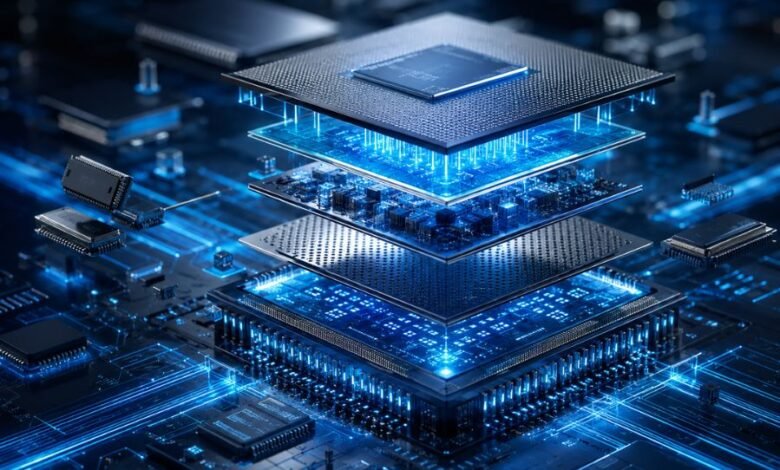
3D Electronic technology is changing the way engineers think about circuits, chips and connected devices. Instead of keeping electronic components on a mostly flat surface, three-dimensional electronics use height and depth to stack, embed or print electrical functions into compact structures. The approach can include vertically stacked semiconductor dies, conductive paths printed on curved objects and fully or partly 3D-printed electronic devices.
The idea matters because modern electronics face growing pressure to become smaller, faster, more power-efficient and better suited to unusual shapes. Advances in semiconductor packaging, additive manufacturing and conductive materials are making these designs increasingly practical. This article explains what 3D electronics are, how they work, where they are already being developed and why the technology could become increasingly important for computing, healthcare, wearables, robotics and manufacturing.
What Does 3D Electronic Technology Mean?
The term 3D Electronic is best understood as a broad description of electronic systems in which circuitry, components or functional materials extend through three-dimensional space rather than existing only on a conventional flat circuit board.
There are several approaches within this field. In semiconductor manufacturing, 3D integration can mean stacking separate dies or functional layers vertically and connecting them through extremely short electrical paths. TSMC, for example, describes its 3DFabric platform as a family of 3D silicon-stacking and advanced-packaging technologies, while Intel uses Foveros technologies to vertically integrate chiplets and active dies.
Another branch involves 3D-printed electronics. Here, conductive, insulating, semiconducting or functional materials can be deposited in carefully controlled patterns to form electrical structures on or inside three-dimensional objects. Research has demonstrated printed displays, sensors, flexible circuits and complex conductive structures using several additive-manufacturing methods.
How 3D Electronic Systems Work
Vertical Integration in Semiconductor Chips
Traditional integrated circuits are mainly developed across the horizontal surface of a silicon die. Three-dimensional integration adds another direction: upward.
Instead of forcing every function onto one large piece of silicon, designers can divide a system into smaller dies or chiplets and connect them vertically. These dies may handle different jobs such as computing, memory, graphics or input/output operations.
Intel’s Foveros Direct technology, for example, is designed to attach chiplets directly to an active base die and create dense die-to-die connections. Intel describes the approach as providing high-bandwidth, low-power interconnects between vertically integrated components.
TSMC follows a related direction through its 3DFabric technologies, including solutions intended for chip-level stacking and advanced packaging. These technologies allow semiconductor designers to combine different functional elements while treating packaging as an important part of the overall system architecture.
Printing Electronics in Three Dimensions
3D-printed electronics take a different route. Instead of primarily stacking completed silicon dies, additive manufacturing places materials where they are required according to a digital design.
A printer may deposit conductive inks to create electrical tracks, polymers to provide structural support and other functional materials for sensors, electrodes or active devices. Multiple deposition processes can sometimes be combined within a single manufacturing workflow.
Research published in Science Advances has demonstrated fully 3D-printed flexible organic light-emitting diode displays, showing that additive techniques can produce more than simple conductive tracks.
This ability to manufacture electrical and structural features together could eventually reduce the distinction between an electronic device’s housing and its circuit architecture.
Key Manufacturing Methods Behind 3D Electronics
Direct Ink Writing
Direct ink writing (DIW) deposits specially formulated materials through a nozzle. Depending on the application, these inks can contain conductive particles, polymers, liquid metals or other functional materials.
The process is particularly useful when electronics need unusual shapes or flexible mechanical properties. Recent research has used direct ink writing for stretchable electronic systems and wearable structures.
Hybrid Bonding
For advanced semiconductor devices, hybrid bonding is becoming an important method for connecting stacked dies or wafers. It creates very dense electrical connections while reducing the distance that signals must travel between functional layers.
In May 2026, imec and EV Group reported wafer-to-wafer hybrid bonding with a 200-nanometre interconnect pitch, targeting future logic-to-logic and memory-to-logic stacking. The development illustrates how aggressively researchers are working to increase vertical interconnect density.
Multimaterial Additive Manufacturing
A functioning electronic product normally requires more than one material. Conductors must carry electricity, dielectric materials provide insulation, and structural materials maintain mechanical strength.
Multimaterial additive manufacturing attempts to integrate these functions during fabrication. Research has demonstrated embedded bulk-metal conductors and vertical vias inside polymer structures, highlighting the possibility of creating electrical connections directly within complex three-dimensional parts.
Why 3D Electronic Technology Matters
Greater Component Density
Using the vertical dimension gives engineers more physical space for electronic functions without simply increasing a device’s footprint.
This advantage is especially valuable in semiconductor systems, where processors, memory and specialised accelerators need increasingly fast communication. Shorter connections between vertically integrated dies can help reduce the distance data must travel.
More Flexible Product Shapes
Traditional printed circuit boards strongly influence the shape of electronic products because they are usually rigid and relatively flat. Three-dimensional manufacturing offers another possibility: the circuit can follow the product.
Conductive elements can potentially be placed along curved surfaces or embedded within structural components. Research has already demonstrated conformal electronics on curved and flexible substrates, including sensors fabricated directly onto unconventional surfaces.
Integration of Different Technologies
A major attraction of 3D integration is heterogeneous integration. Different dies do not necessarily need to perform the same function or use exactly the same architecture.
A system can be partitioned into specialised functional layers and then interconnected. Imec’s work on CMOS 2.0, for example, examines increasingly fine 3D interconnections for combinations such as logic-to-logic and memory-to-logic stacking.
Where 3D Electronics Could Have the Greatest Impact
AI and High-Performance Computing
Artificial intelligence and high-performance computing require enormous quantities of data to move between processors and memory. This makes interconnect efficiency a major design issue.
Advanced packaging and 3D stacking are therefore becoming closely connected with high-performance system development. TSMC identifies high-performance computing among the applications supported by its advanced 3D integration technologies, while Intel positions its advanced packaging technologies for both client and data-centre applications.
Wearable and Stretchable Electronics
Electronics worn on the body need to cope with bending, stretching and irregular surfaces. Three-dimensional printing can produce structures designed around these movements rather than forcing a rigid circuit onto them.
A 2026 Nature Communications study demonstrated 3D-printed multilayer stretchable electronics with three-dimensional interconnections. The researchers reported devices capable of substantial mechanical deformation and demonstrated applications including physiological monitoring.
Such research points toward more integrated health-monitoring systems, electronic skins and human-machine interfaces.
Robotics and Smart Structures
Robots increasingly require sensors, wiring and electronic control systems distributed through complex mechanical structures. Printing or embedding electronics directly within components could simplify some designs and make new shapes possible.
Multimaterial 3D printing research has already demonstrated soft robotic structures containing integrated electronic or fluidic functions, indicating how additive manufacturing can combine mechanical and electrical design more closely.
Medical and Biomedical Devices
Three-dimensional electronics may also help produce sensors and interfaces that conform more naturally to biological structures.
Researchers have demonstrated conformal printed sensors on medical-device surfaces, while advances in flexible electronics continue to investigate interfaces capable of operating safely while bending or stretching.
Commercial adoption, however, requires much more than laboratory performance. Medical systems must meet demanding requirements for reliability, manufacturing consistency, safety and regulatory approval.
Major Challenges Facing 3D Electronic Manufacturing
Despite its advantages, three-dimensional integration creates difficult engineering problems.
Heat management is one of them. Placing active components close together can make thermal design more complicated, especially in high-performance processors. Manufacturing defects are also more difficult to manage when several valuable layers or dies are combined into one system.
Alignment presents another challenge. Advanced semiconductor bonding depends on extremely precise positioning of tiny interconnects. As pitches become smaller, surface preparation, wafer deformation and overlay accuracy become critical manufacturing concerns. Imec’s hybrid-bonding research specifically identifies alignment and surface control as major issues when scaling 3D connections.
Printed electronics face different obstacles. Conductive materials must offer reliable electrical performance while remaining compatible with printing, curing, flexible substrates and other materials. Manufacturers also need repeatable processes that can move from impressive laboratory prototypes to large production volumes.
What Is Changing in 3D Electronics in 2026?
The field is advancing from multiple directions rather than following a single technology path.
In semiconductor manufacturing, research is pushing toward finer hybrid-bonding connections and increasingly sophisticated vertical system architectures. Imec’s 2026 work on 200-nanometre-pitch wafer-to-wafer hybrid bonding is one example of this continuing effort.
Additive electronics are progressing at the same time. A 2026 Science Advances study examined three-dimensional printing of nanomaterial-based electronics, reflecting continued research into freeform electronic architectures. Another 2026 study demonstrated multilayer stretchable electronics produced through additive manufacturing.
These developments suggest that the future of 3D electronics will not belong to a single manufacturing process. Semiconductor stacking, additive manufacturing, flexible materials and advanced packaging are likely to solve different problems while increasingly overlapping.
Conclusion
3D Electronic technology represents a shift from treating electronics as mainly flat circuits toward designing functional systems throughout three-dimensional space. In advanced chips, vertical stacking can bring specialised dies closer together and support dense connections. In additive manufacturing, conductive and functional materials can be printed onto curved surfaces or incorporated directly into flexible and structural parts.
The technology still faces significant challenges involving heat, manufacturing yield, materials, alignment, durability and large-scale production. Yet research and commercial semiconductor development are moving rapidly. As computing systems become more complex and devices need to fit more naturally into products, clothing, robots and specialised equipment, three-dimensional electronic design is likely to become an increasingly important part of modern engineering.
(FAQs)
What is 3D Electronic technology?
3D Electronic technology refers broadly to electronic circuits, components or functional materials arranged, stacked, printed or embedded in three dimensions rather than being limited to a conventional flat circuit layout.
Is 3D electronics the same as 3D printing?
No. 3D printing is one method used to manufacture certain three-dimensional electronic structures. The wider field also includes semiconductor die stacking, hybrid bonding, conformal electronics and other forms of vertical integration.
What are 3D electronic chips?
They are semiconductor systems in which multiple dies, chiplets or functional layers are vertically integrated and electrically connected. Technologies developed by companies such as Intel and TSMC are examples of advanced approaches to 3D semiconductor integration.
Can electronic circuits really be 3D printed?
Yes. Researchers have demonstrated printed conductive structures, sensors, flexible displays and multilayer electronics using additive-manufacturing techniques. However, capability and manufacturing maturity vary considerably depending on the device and materials involved.
What is the future of 3D electronics?
Current research points toward denser stacked chips, improved chiplet integration, flexible and wearable devices, conformal sensors and more sophisticated multimaterial printing. Progress will depend on solving manufacturing, thermal, reliability and materials challenges.